


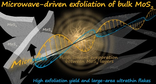
Microwave-driven exfoliation of MoS2 produces large flakes with high yields
23.03.2023
- A team of researchers have tested a novel method for exfoliating MoS2 with large lateral sizes and with high yield.
- The microwave-assisted exfoliation yields 50 times more flakes than those obtained by ultrasonication and gives a material quality comparable to mechanical exfoliation.
- This fast process requires minimal processing and holds promise to enable new applications in electronic and photonic devices.
Madrid, March 23rd, 2023. A team of researchers has developed a new method for exfoliating MoS2 flakes that produces very large and very thin flakes with high yield. MoS2 is a transition metal dichalcogenide, a material interesting in the field of electronics for its wide range of physical properties from semimetallic to semiconductors, superconductors or insulators, depending on its dimensions. The number of stacked layers is crucial in determining these properties. Monolayer MoS2, for instance, exhibits a direct bandgap of 1.90 eV, while bulk 2H-MoS2 presents an indirect bandgap of 1.23 eV. These tailorable properties make them ideal candidates for applications. However, obtaining large area, high-quality MoS2 flakes has proved challenging.
Existing liquid-phase exfoliation methods have low yields and often result in broad thickness distributions, making it difficult to obtain monolayer and few-layered 2H-MoS2. In an attempt to improve yields, researchers have explored other techniques, including ball milling, electrochemical exfoliation, and fluid dynamics exfoliation. However, these methods have scalability problems or produce metallic 1T- MoS2, which has different properties and applications.
The team, led by Professors Víctor Sebastián and Jesús Santamaría from the Institute of Nanoscience and Materials in Zaragoza (INMA, CSIC-UNIZAR), and Professor Emilio M. Pérez from the Madrid Institute of Advanced Studies in Nanoscience, both in Spain, have tested a novel microwave-assisted method for exfoliating MoS2 flakes. They found that the method produced well-exfoliated material with lateral sizes comparable to those obtained by mechanical exfoliation. The yield of the process is roughly 50 times greater than ultrasonication exfoliation methods. It gives a material quality comparable to mechanical exfoliation, whose flakes are similar to those obtained by this method but with an incomparably higher yield (mechanical exfoliation is actually carried out flake by flake!). The process is fast, taking only a few minutes, and requires minimal processing.
|
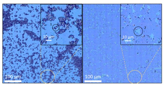
The lateral dimension of the MoS2 flake (highlighted in 1 and 2) is larger than 5 microns. |
The method has the potential to enable new applications of MoS2 in electronic and photonic devices. It has been applied to MoS2, but it could be used to exfoliate any material with high microwave absorption capabilities, being a versatile approach in the area of emerging 2-dimensional (2D) materials. The researchers plan to investigate the method further, exploring its scalability and potential applications in more detail.
What is the most exciting thing about your results?
EMP and VS: To me, it's the lateral size of the flakes. 2D materials have to be very thin, of course, and that is the whole point of exfoliation methods, but it is often overlooked that, for most applications, you want them to be large in lateral size, too. But obtaining flakes which are large and thin at the same time, as well as with high yield, is not easy, as all exfoliation methods come down to adding some form of energy to the bulk material, to overcome the van der Waals interactions between layers. And it is difficult to prevent that same energy causing lateral damage at the same time. Our method manages to use microwaves to evaporate solvent molecules between layers, creating a high pressure between them very quickly, so that they can be separated, but are not damaged.
What are the potential real-life applications of the method?
EMP and VS: 2D materials in general, and transition-metal dichalcogenides in particular, are promising for a lot of technologies (sensors, electronics, etc.) but obviously it all starts with making these materials with good quality, ideally in large quantities, and cheaply. This is where our work can contribute. It is not a step towards a new specific technology, but rather a tool to help all of the hope deposited on 2D materials become a reality.
This work is a result of a successful collaboration among scientists from the Madrid Institute for Advanced Studies in Nanoscience (IMDEA Nanociencia, Madrid), and the Institute for Nanoscience and Materials of Aragón INMA (Universidad de Zaragoza-CSIC). It has been partially funded by the ERC-PoC grant 842606, ERC-AdG 742684 and the Comunidad de Madrid project MAD-2D, as well as the Severo Ochoa Centre of Excellence seal awarded to IMDEA Nanociencia in 2017.
Reference
Ramiro Quirós-Ovies, María Laborda, Natalia Martín Sabanés, Lucía Martín-Pérez, Sara Moreno-Da Silva, Enrique Burzurí, Víctor Sebastian, Emilio M. Pérez, and Jesús Santamaría. Microwave-driven exfoliation of bulk 2h- MoS2 after acetonitrile prewetting produces large-area ultrathin flakes with exceptionally high yield. ACS Nano (2023). DOI: 10.1021/acsnano.3c00280
![]() Open access to the full text (IMDEA Nanociencia Repository): https://repositorio.imdeananociencia.org/handle/20.500.12614/3283
Open access to the full text (IMDEA Nanociencia Repository): https://repositorio.imdeananociencia.org/handle/20.500.12614/3283
Contact
Prof. Emilio M. Pérez
emilio.perez [at]imdea.org
Chemistry of Low Dimensional Materials Group https://nanociencia.imdea.org/chemistry-of-low-dimensional-materials/home
Twitter: @emiliomperezlab
Victor Sebastian
This email address is being protected from spambots. You need JavaScript enabled to view it.
IMDEA Nanociencia Dissemination and Communication Office
divulgacion.nanociencia [at]imdea.org
Twitter: @imdea_nano
Facebook: @imdeananociencia
Instagram: @imdeananociencia
Source: IMDEA Nanociencia