


Direct after-fabrication tailoring of MoS2-FET transistors
08.07.2019
 |
|
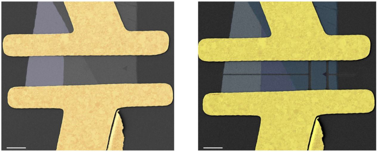
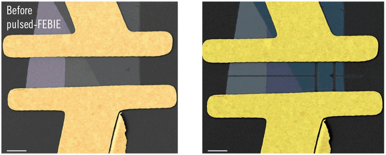
MoS2 FET device before and after the pulsed-focused electron beam induced etching (pulsed-FEBIE) nanopatterning, with a tailored conduction channel. Image: Fernando J. Urbanos. |
The fabrication of electronic devices from exfoliated 2D materials can be tricky. The group of Daniel Granados at IMDEA Nanociencia have engineered a solution that consist on the after-fabrication tailoring of MoS2-FET transistors using pulsed-focused electron beam induced etching.
Transition metal dichalcogenides are discrete 2D atomically thin layers bound together by Van der Waals forces. These materials exhibit thickness-dependent variations in their physical properties that can be exploited in distinct optoelectronic applications. For example, the band structure of molybdenum disulphide (MoS2) has a direct bandgap of 1.8 eV in a single layer that narrows down with thickness, being 1.2 eV indirect bandgap in bulk.
The atomically thin layers of MoS2 can be separated by micromechanical exfoliation, nonetheless the fabrication of optoelectronic devices from mechanically exfoliated MoS2 is an intricate process. The geometry of the device is limited in all cases by the shape of the exfoliated flake, even when a deterministic stamping method is employed. Even when using CVD (chemical vapour deposition) techniques the device fabrication is hindered by the material growing in islands with reduced sizes and different physical properties.
Thus, developing techniques to tailor the device geometry after the fabrication steps are completed is of great interest. The group of Prof. Daniel Granados at IMDEA Nanociencia has come to a smart solution to modify the geometry of several field effect transistors (FET) fabricated out of exfoliated MoS2. The proposed method uses a variation of the Focused Electron Beam Induced Etching (FEBIE) with a pulsed electron beam. The beam scans the surface into a designed geometry employing a pattern generator, modifying of the conduction channel between the source and the drain of the transistor and allowing a tailor-made device performance.
 Prof. Granados likes to use the hydrodynamic analogy: “It is like turbulent flow, after passing certain apertures it becomes laminar; our tailored conduction channels allow the electrons passing by areas of the MoS2 flakes with identical properties”.
The effect of this modification method has been studied further to verify the performance of the modified devices. Granados’ group has found that 90% of the devices work after the nanopatterning. Further, they studied the shift that is produced from clear heavily N-type doping towards intrinsic or lightly P-type, and attributed this change to sulphur vacancies created when etching. The doping shift was confirmed by photoluminescence and Raman spectroscopy studies.
This method presents several advantages compared to those that use several fabrication steps. First, it combines patterning and etching into a single step instead of having a two-step nanofabrication process. Second, it allows electronic and optical characterization before and after the tailoring step in a simple scheme. Last, the pulsed-FEBIE is a chemical method that has an electron beam energy lower than other studies (2.5 kV) that reduces the sample damage and prevents the distortion of the MoS2 lattice. Because of these advantages, the “nanoscissors” proposed by Granados et al. are a remarkable alternative to the expensive and time-consuming nanofabrication techniques and have a great potential for the after-fabrication tailoring of the electrical and geometrical properties of electronic and optoelectronic devices.
This research is a collaboration between researchers at IMDEA Nanociencia (Spain), University of Hamburg (Germany), University of Lancaster (United Kingdom) and Autónoma University of Madrid (Spain), and has been partially funded by Comunidad de Madrid, Spanish Ministry of Economy and Competitiveness and the European Commission (Graphene Core), as well as the Severo Ochoa Programme for Centres of Excellence awarded to IMDEA Nanociencia (2017-2021).
Reference:
F. J. Urbanos et al. Electrical and geometrical tuning of MoS2 field effect transistors via direct nanopatterning. Nanoscale. 2019.
DOI: 10.1039/C9NR02464F
Contacto
Daniel Granados
daniel.granados [at]imdea.org
http://nanociencia.imdea.org/quantum-nanodevices/group-people
Twitter: @danieldanigran
IMDEA Nanociencia Outreach Office
This email address is being protected from spambots. You need JavaScript enabled to view it.
+34 91 299 87 12
Twitter: @imdea_nano
Facebook: @imdeananociencia
Source: IMDEA Nanociencia