




A niobium-telluride material reveals an unexpected structure when reduced to a single atomic layer
29.10.2026
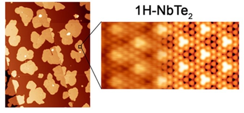
NbTe₂ islands and a close-up of the crystal structure. Credit: Manuela Garnica
- Researchers at IMDEA Nanociencia have identified a new two-dimensional phase of NbTe₂ that does not exist in bulk.
- The study reveals a periodic rearrangement of the electronic charge at low temperatures and opens new avenues for investigating the fundamental properties of two-dimensional quantum materials.
| Tweet |  |
Press release download |
Madrid, 29th, October, 2026. Transition-metal dichalcogenides are a family of materials with electronic and structural properties of great interest to nanoscience research. Among them, selenium- and sulfur-based compounds have received the most attention, while those containing tellurium exhibit less-explored behaviors and distinct characteristics. One of the phenomena these materials can exhibit is charge density waves (CDWs), a periodic rearrangement of the electron distribution that gives rise to new electronic states. However, reducing these materials to a single atomic layer can drastically alter their structure and properties, and the behavior of niobium ditelluride (NbTe₂) under these conditions continued to raise questions.
A research team led by IMDEA Nanociencia has succeeded in synthesizing and characterizing two-dimensional islands of NbTe₂ with a type-1H hexagonal crystal structure, a metastable phase not observed in bulk material. To obtain them, the team used molecular beam epitaxy on graphene grown on an iridium surface. Using spectroscopy and tunneling microscopy techniques, angle-resolved photoemission spectroscopy (ARPES), and first-principles theoretical calculations, the researchers confirmed the structure and metallic nature of this phase.
Furthermore, measurements taken at low temperatures revealed a modulation of the charge density with a periodic 4 × 4 pattern, related to an instability in the crystal lattice vibrations.
“This was not what we expected from this material, because in three dimensions it has a type-1T structure, not this hexagonal 1H phase,” explains Manuela, the study’s lead author. The finding is particularly significant because it demonstrates that a material’s properties can change when confined to two dimensions. Furthermore, tellurium can give rise to electronic states that do not necessarily appear in its equivalent compounds with selenium or sulfur. Charge density waves are an example of how electrons can collectively reorganize and generate correlated states. “This work adds a new piece to the scientific debate on how matter reorganizes itself on a two-dimensional scale and helps us better understand these materials at a fundamental level,” notes the researcher. As a next step, the team plans to study the material at even lower temperatures, around 1 K, to explore the existence of superconductivity and how it might compete with the reorganization of the electronic charge.
The results have been published in the journal ACS Nano. The work is led by researchers at IMDEA Nanoscience, where the ARPES measurements were conducted, with the theoretical analysis carried out in collaboration with the Barcelona Institute of Materials Science (ICMAB-CSIC). The research contributes to expanding our understanding of two-dimensional materials and their electronic phases, a field of interest for understanding and exploring new properties of matter at the nanoscale.
IMDEA Nanociencia has been accredited as a Severo Ochoa Center of Excellence, a distinction awarded by the State Research Agency for the period 2026–2031. This publication is part of the “Severo Ochoa Excellence” grant CEX2025-001660-S, funded by MICIU/AEI/10.13039/501100011033.
Glossary:
- Transition-metal dichalcogenides: A family of materials with electronic and structural properties of great interest in nanoscience, whose behaviors change drastically when reduced to a single atomic layer.
- Charge-density waves: A physical phenomenon consisting of a periodic rearrangement of the electron distribution, giving rise to new electronic states at low temperatures.
Reference:
Noor ul Ain, Alireza Amiri, Fabian Calleja, Beatriz Muñiz Cano, Archit Dhingra, Riccardo Rurali, Amadeo L. Vázquez de Parga, Rodolfo Miranda, Miguel A. Valbuena, Enric Canadell, Jose Angel Silva-Guillén, Manuela Garnica; Unexpected 4 × 4 Charge Density Wave in 1H-NbTe2 Monolayer. ACS Nano 20 October 2026; 20 (41): 27706–27715. https://doi.org/10.1021/acsnano.6c07014
 https://hdl.handle.net/20.500.12614/4295
Contact:
Manuela Garnica
This email address is being protected from spambots. You need JavaScript enabled to view it.
Topological Surfaces States in Quantum Materials Group
https://www.nanociencia.imdea.org/nanoscale-imaging-of-2d-materials/group-home
IMDEA Nanociencia Dissemination and Communication Office
This email address is being protected from spambots. You need JavaScript enabled to view it.
+34 91 299 87 12


Source: IMDEA Nanociencia.
The IMDEA Institute of Nanoscience is a young interdisciplinary research center in Madrid, Spain, dedicated to the exploration of nanoscience and the development of nanotechnology applications for innovative industries.